0 Introduction
In order to improve the whole efficiency of the electronic equipment, the search for more efficient soft switching technique has been developed. For switch such as IGBT,the zero- current switching(ZCS) and zero-current transition(ZCT)technology have been frequently used, because this method can reduce the current rapidly when IGBT turns off, therefore reducing the energy loss caused by the tail current [1][2][3][4][5].
But the zero-current switching circuit that mostly used is not input-out-isolated, so the application in the practice has not been generalized. This paper proposed the ZCS technique realized by the half bridge converter, both the main switch and auxiliary switch in the topology work in soft switching state, the turn-on current stress and turn-off voltage stress is small.
1 Operational Principles
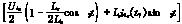
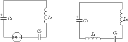
Fig.1 shows the circuit diagram of the half-bridge converter. In the schematic, Lr1 to Lr4 are resonant inductors, the Cr is resonant capacitor, S1 and S2 are main switches, S3 and S4 are auxiliary switches, D1 to D4 are anti-parallel diodes in the switches, Cs1 to Cs4 are snubber-capacities. The circuit is the conventional half bridge topology incorporating the auxiliary resonant tank that composed of switches S3 and S4. The zero current switching state can be obtained by controlling the work sequence of the switches. Fig.2 is the theoretical waveforms when the converter in steady-state operation.
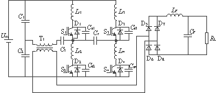
Fig.1 Schematic of the ZCS PWM half-bridge converter
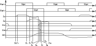
Fig.2 the main ideal waveform
The ideal analyses are given for all modes of the circuit, there are some differences between the theoretical analyses and practical condition because the following assumptions are made:
1)The link capacitor C1 and C2 in the half-bridge are so large that the voltage of the capacitors can be treated as a constant in each switching period.
2)The capacitor C3 is so large that there is little voltage reduction in C3.
3)The output filter inductor Lf is large enough that the current through it can be treated as a constant in each switching period.
4)The S1,S2,S3 and S4 are ideal switches.
5)The snubber-capacity Cs1,Cs2,Cs3 and Cs4 are much smaller than the resonant capacity Cr, so the influence on the resonance can be disregarded.
Additionally, the parameter meets the following:
6)The value of the leakage inductor Lk of the transformer is much larger than that of the resonant inductor.
7)The value of Lr1,Lr2,Lr3 and Lr4 is Lr.
8)The value of Cs1,Cs2,Cs3 and Cs4 is Cs.
9)The link capacitor C1 and C2 have the same values of C.
Just as conventional ZCS DC-DC converter circuit, the circuit can easily realize ZCS in light load condition. So the research and experiment in this paper are mainly concentrated in heavy load condition. To heavy load condition, the work process of the circuit can be sorted as following nine models:
Model 1〔 t0~t1〕 At t0, the switch S1 turns on, but the power is not delivered to the load because the transformer is shorted, the electric energy is only transfer to the leakage inductor Lk and resonant inductor Lr. So the current increase gradually from zero to Io/n (the n is the turn ratio of the transformer), the turn-on state of switch is zero current. The current conducting through S1 increases linearly with the slope of Uin/2(Lk+Lr), therefore the time interval of this model is given by
t1-t0=2(Lr+Lk)Io/(nUin) (1)
Model 2〔 t1~t2〕 At t1, when the current through S1 is equal to Io/n, the power energy is delivered to the load, the circuit is in half-bridge converter PWM state. Then the current through S1 maintains to be Io/n.
Model 3〔 t2~t3〕 At t2, the auxiliary switch S3 turns on in zero-current state. The resonant tank composed of Lr1, Lr3 and Cr begins to work. If the voltage of Cr at t2 is uCr(t2), the voltage of Cr can be expressed as
uCr=uCr(t2)cos〔 ω 1(t-t2)〕 (2)
The current of Lr1 can be expressed as
iLr1=Im1sin〔 ω 1(t-t2)〕 (3)
where the resonant frequency ω 1 is given by
ω 1= (4)
(4)
The maximum current of the Lr1 can be given by
Im1=uCr(t2)/ZLC (5)
The impedance of the resonant ZLC can be given by
ZLC= (6)
(6)
Model 4〔 t3~t4〕 At t3, the current through the resonant tank increases to Io/n, the current through S1 decreases to zero, the anti-parallel diode begins to work, because the current through resonant tank increases from zero, according to
i(t3)=Io/n (7)
The time interval can be derived from
t3-t2= (8)
(8)
Model 5〔 t4~t5〕 At t4, when turning off the S1, the S1 is in zero-current state, but the anti-parallel diode is still in conducting state. The current through resonant tank decreases from Im1 to Io/n, The total time interval of model 4 and model 5 is
t5-t3=2 (9)
(9)
By the equation (2) and (9), the voltage of Cr at t5 can be expressed as
uCr(t5)=- UCr(t2) (10)
(10)
Model 6〔 t5~ t6〕 At t5, the current of resonant tank decreases to Io/n, the diode D1 turns off naturally, then the current through the resonant tank will keep to be Io/n, the voltage of S1 begins to increase, while the voltage of S2 to decrease.Because the capacitor discharges in constant current, so the voltage of resonant capacitor can be given as
uCr(t)- uCr(t5)=  (11)
(11)
From the equation(11) we can see that the voltage value of resonant capacitor increases gradually, at t6, to Uin/2. From equation (10) and (11), we know that the time interval of this model can be expressed as
t6-t5=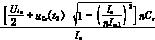 (12)
(12)
Model 7〔 t6~ t7〕 At t6, the voltage of Cr begins to increase from Uin/2, the rectifier composed of D5 to D8 begins to conduct, the voltage of S2 continues to decrease. The resonant network is composed of inductor Lr3, resonant capacitor Cr and leakage inductor Lk, and the network cooperation with link capacitor C1, the initial state of the resonant network is
iLr3(t6)= (13)
(13)
uCr(t6)= (14)
(14)
Therefore this model should meet the following equation:
uCr(t)= cos〔 ω 2(t- t6)〕 +
 sin〔 ω 2(t- t6)〕 (15)
iLr(t)= cos〔 ω 2(t- t6)〕 -
 sin〔 ω 2(t- t6)〕 (16)
where
ω 2= (17)
(17)
At t7, when the voltage of Cr is Vin, the D2 begins to work, the voltage of the leakage inductor is fixed at (Lk+ Lr)Uin/Lk. From equation (15) and (16). We can see that the time interval of model 7 can be given by
t7-t6= arctan
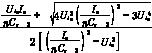 (18)
(18)
Model 8〔 t7~ t8〕 At t7, the voltage of S2 decreases to zero, the anti-parallel diode D2 begins to work, the current through the transformer will be reduced to zero by the capacitor C2.
In this model, the current of Lr3 should meet the following equation:
iLr3(t)=iLr(t7)cosω 3t-  sinω 3t (19)
where
ω 3= (20)
(20)
The current of leakage inductor can be given by
ik(t)=
 -
- iLr(t7) (21)
The voltage of Cr should meet the following equation:
uCr(t)= ×
×  (22)
(22)
The time interval of this model can be given by
t8- t7= (23)
(23)
Model 9〔 t8~ t10〕 At t8, the current through the transformer is zero. The resonant tank composed of Cr,Lr3 and Lr2 will begin to work, and the current through Lr3 will change the direction. At t9, when turning off S3, the S3 is in ZCS model. After half of the resonant period, the current of Lr3 decreases back to zero and the anti-parallel diode D3 turns off natu rally. The time interval of this model can be given by
t10- t8= (24)
(24)
The work process of S2 is accordant with above, so in this paper the work process of S1 is mainly discussed.
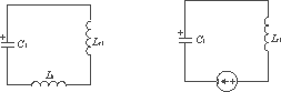
( a) 〔 t0~ t1〕 ( b) 〔 t1~ t2〕
( c) 〔 t2~ t3〕 ( d) 〔 t3~ t5〕
( e) 〔 t5~ t6〕 ( f) 〔 t6~ t7〕
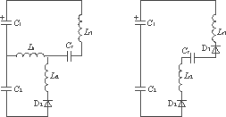
( g) 〔 t7~ t8〕 ( h) 〔 t8~ t10〕
Fig.3 The equivalent circuits of the work process by S1
2 The Discussion to the Circuit Model
2.1 The Duty Ratio Loss
The duty ratio loss is concentrated in time interval t0 to t1, therefore the duty ratio loss is
Dloss= (25)
(25)
where Ts is the switch cycle period.
2.2 Minimum Duty Ratio
To ensure soft switching off, there should be enough time for the current of S1 to decrease to zero before the switch turns off. From model 3, equation (8), we can deduce the minimum duty ratio is
Dmin= (26)
(26)
2.3 Soft Commutation Conditions
1)From the analysis for model 4, 5 and equation (8) and (9), we can see that, if there is enough time for S1 to realize turning at zero current, the maximum current of the resonant network must meet the following expression:
Im1=  (27)
(27)
2)If the output current Io is small, and the Io meet the following expression:
 < Uin (28)
From equation (15), we know that the voltage of Cr will not increase to Uin, the D2 would not conduct, the time interval of model 7 would delay until the current of the Lk decreases to zero, therefore the model 8 would disappeared. But still the IGBT is switched in ZCS, and the D3 turns off naturally.
3)From the above analysis to topology, we can see that in the topology, if the maximum current is larger enough to meet the expression (27), and the time t4 correspended to main switch turning off satisfies the following condition:
t2+ < t4< t2+
 (29)
(29)
and the time t9 correspended to auxiliary switch turning off meets the following condition:
t8< t9< t2+ (30)
(30)
then the main switch and auxiliary switch are all well in zero-current switch. The resonant inductors Lr1 to Lr4 do not only slow down the increasing rate of the current when switching on, but also realize soft-switch when the switch turns off. This is realized through making the anti-parallel diode conduct by the resonant network.
3 Experiment Results
To verify the operation and the performance of the proposed improved half-bridge converter, the 1 kW prototype has been implemented, the following are main parameters
Input voltage Uin, 232 V;
Output voltage, 80 V;
Output resistance value, 6 Ω ;
Switching frequency fs, 80 kHz;
Leakage inductor value, 5 μ H;
The resonant inductor, 1 μ H;
Resonant capacitor is 72 nF.
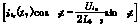
Fig.4 is the voltage and current waveform when the switch working. Fig.4(a) is for the main switch and fig.4(b) for auxiliary switch. From the waveform presented, we can see that main switch and auxiliary switch are well done in zero-current switch, and the stress of the current and voltage is small.

(a) The voltage and current waveform of main switch
(The scale of current is 5A/div, that of time is 1μ s/div)
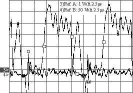
(b) The voltage and current waveform of auxiliary switch
(The scale of current is 10A/div, that of time is 2.5μ s/div)
Fig.4 The main experimental waveform
(The abscissa is time, and the ordinate is voltage and current, the scale of the voltage is 50V/div and the voltage wave form is marked by “ □ ” )
4 Conclusion
From the theoretical analysis and experiment result, we can see that the topology has following feature:
— Because the resonant inductors Lr1 to Lr4 are in series with switches, they cooperate with leakage inductor Lk that slow down the change rate of the current. Therefore the current stress has been reduced when the switches turn on.
— The resonant inductors Lr1 to Lr4 finish the soft switch in cooperation with the Cr.
— The anti-parallel diodes work in soft-switch state.
— The topology is not strict with the leakage inductor.
— The topology is adapted to improve the IGBT work frequency.